pin과 via 사이에 copper flood가 완전히 채워지지 않을 때 방안으로 두 가지 섹션이 있습니다.
첫 번째 섹션에서는 copper plane outline width 와 copper hatch grid을 줄임으로써 via 사이의 copper flooding을 보여줍니다.
두 번째 섹션에서는 smoothing radius 을 줄임으로써 via 사이의 copper flooding을 보여줍니다.
1️⃣Copper plane outline width
pin과 via 사이에 copper를 빈 부분 없이 flood하는 가장 일반적인 방법은 copper plane outline width와 copper hatch grid 설정을 줄이는 것입니다.
1. Copper plane flood를 하기 위한 pcb file을 open 합니다.
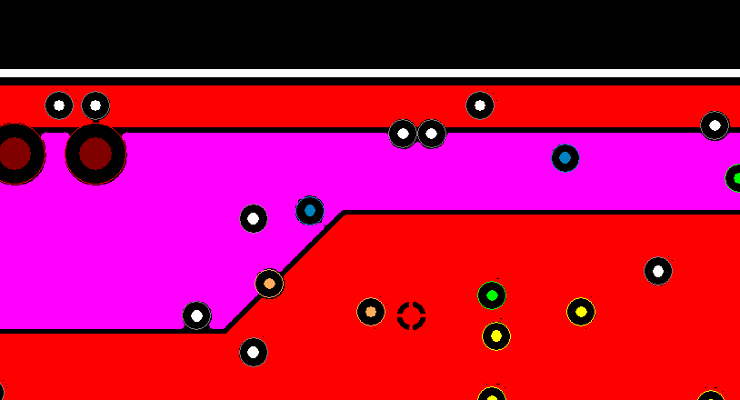
2. Tools > Copper Plane Manager를 사용하여 layer를 채우고 layer에 큰 빈 공간이 있는 것을 확인합니다.
3. modeless command PO를 입력하고 Enter 키를 눌러 filled coppe가 더 이상 존재하지 않도록 pour outline mode를 전환한 후에 copper plane shape을 선택하고 마우스 오른쪽 버튼을 클릭한 다음 속성을 선택합니다
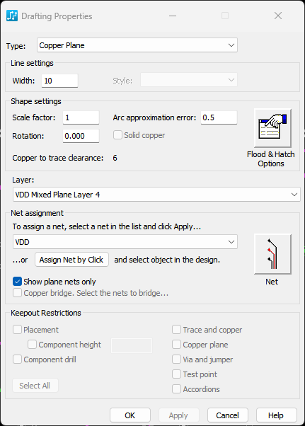
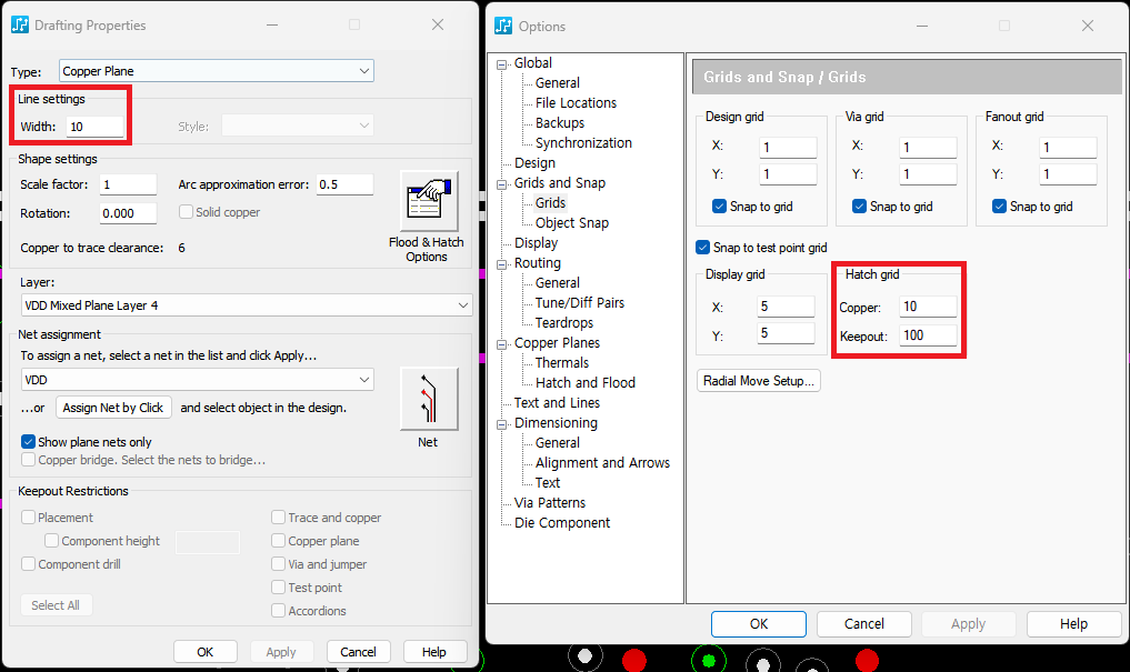
4. 윤곽선 너비를 기본 10mil에서 5mil로 변경 후 Tools > Options > Grids and Snap > Grids로 이동합니다.
Copper Hatch grid 설정을 10mil에서 5mil로 변경하고 확인을 클릭합니다.
5. Tools > Copper Plane Manager로 이동하여 copper planes을 flood합니다.
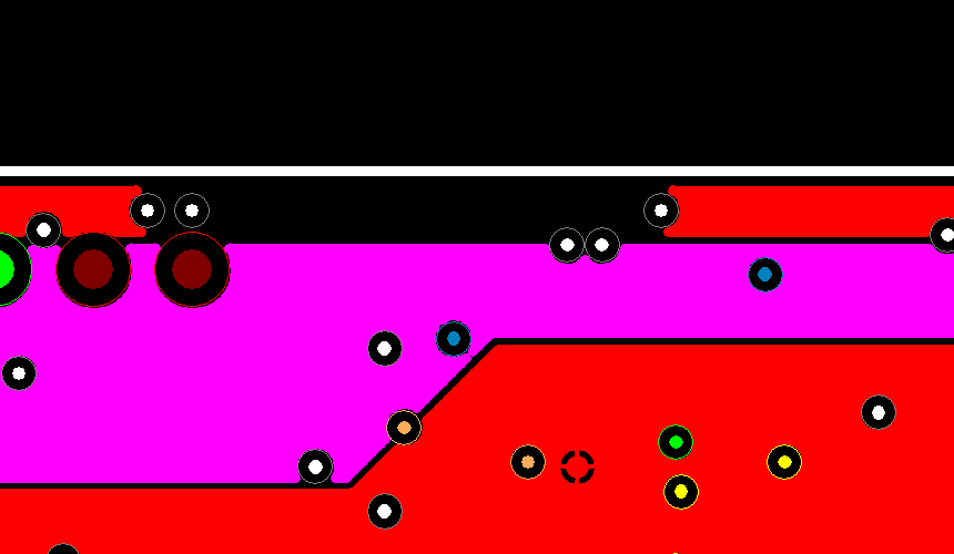
빈 공간이 채워져서 flooding된 모습을 확인할 수 있습니다.
2️⃣Copper Flood Smoothing Radius
경우에 따라 copper plane smoothing radius가 핀 사이 copper floods방식에 영향을 줄 수 있습니다. smoothing radius는 copper plane corners을 제어합니다.
1. Copper plane flood를 하기 위한 pcb file을 open 합니다.
하기 디자인에는 이미 copper width 값과 copper hatch grid가 5mil로 설정되어 있지만 smoothing radius는 0.5로 설정되어 있습니다.
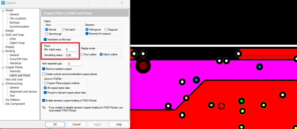
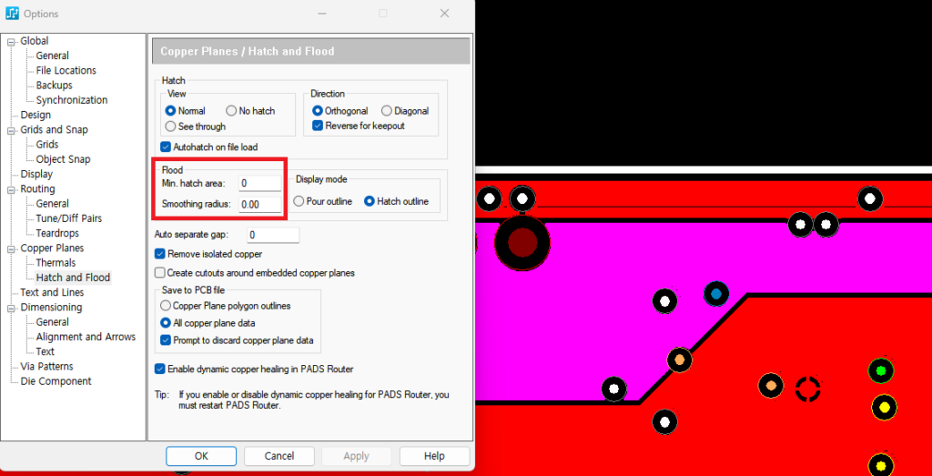
2. Tools > Options > Copper Planes > Flood and Hatch로 이동하여 smoothing radius 0으로 설정하고 확인을 클릭합니다.
Tools > Copper Plane Manager를 사용하여 plane을 다시 채웁니다.